20+ digital pll block diagram
Frequency is scaled by the use of counters. Software-controllable clickless mute.
A Block Diagram Of The Proposed Digitally Implemented Phase Locked Loop Download Scientific Diagram
Join us at AutoSens Brussels.

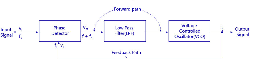
. A PLL is a truly mixed-signal circuit involving the co-design of RF digital and analog building blocks. January 2022 DS12991 Rev 4 194 STM32G030x6x8 Arm Cortex-M0 32-bit MCU up to 64 KB Flash 8 KB RAM 2x USART timers ADC comm. A non-linear negative feedback loop that locks the phase of a VCO to a reference signal.
323 Audio PLL Clock 20 33 Analog Peripherals 20 331 Analog-to-Digital Converter ADC 20 332 Digital-to-Analog Converter DAC 21 333 Temperature Sensor 21 334 Touch Sensor 21 34 Digital Peripherals 22. Since phase noise is multiplied up from the PFD reference frequency at a rate of 20 logN reducing N by a factor of 2 will improve system phase noise by 3 dB ie doubling the PFD frequency reduces phase noise by 10 log2. Analog automatic level control ALC Microphone bias reference voltage.
DS40001729 PIC16LF17059 Data Sheet 1420-Pin Flash 8-bit Microcontrollers. 18 V to 365 V. This is information on a product in full production.
4 CD4046B Phase-Locked Loop. Applications include generating a clean tunable and stable reference LO frequency a process referred to as frequency synthesis. The PLL structure consists of a low-power linear VCO and two.
The benefit of using an external reference PLL LNB is that the indoor reference oscillator is easier to maintain at a stable constant temperature. System Block Diagram Introduction MPC5744P Data Sheet Rev. Integer-N PLL Compared to the analog techniques used in the infancy of frequency synthesis the modern PLL is now a mostly digital circuit.
Digital audio serial data IO. Pll applications pll ic 565. Analog-to-digital converter ADC 4 modules with 12-bit ADC each with 16 channels 25.
This is information on a product in full production. A Versatile Building Block for Micropower Digital and Analog Applications 3 CD4046B PLL Technical Description Figure 2 shows a block diagram of the CD4046B which has been implemented on a single monolithic integrated circuit. The transducer in our case a microphone converts sound into an electrical signal.
Block Diagram Cryptographic Hardware Acceleration RTC Wi-Fi Main CPU JTAG ULP co-processor PMU RTC memory. Layout-Design-Rules Digital-CMOS-Design CMOS-Processing-Technology planar-process-technologySilicon-Crystal-Growth Twin-tub-Process Wafer-Formation-Analog electronic circuits is exciting subject area of electronics. Such PLL LNBs have in internal crystal oscillator or rely on an external 10 MHz reference signal sent up the cable by the indoor receiver.
Glad you found it useful. The wireless communications industry is the digital PLL circuit. May 20 2020 at 926 AM.
PLL LNBs are more expensive. I 2 C and SPI control interfaces. While there are some benefits to using other synthesis techniques they are outside the scope of this document and will not be discussed here.
17 35 40 71 94 96 132 137 B1 G7 G8 G9 G10 G11 H7 H8 H9 H10 H11 J7 J8. DS41391 PIC16LF18261827 Data Sheet 182028-Pin Flash Microcontrollers. Block diagram of a digital signal processing system DSP The first step is to get an electrical signal.
Analog and digital IO. 61 112017 NXP Semiconductors 5. DS40001722 PIC16LF17037 Data Sheet 1420-Pin Flash 8-bit Microcontrollers Note.
For other small form-factor package availability and marking information please visit. Onsemi as the lead sponsor of this event will showcase its intelligent sensing solutions for ADAS autonomous driving in-cabin viewing and LiDAR applicationsDont miss the chance to attend our keynote and meet with our experts to find the right solution for your design challenges. Block diagram of a DSP system.
Enter the email address you signed up with and well email you a reset link. PLL supporting input clocks from 8 MHz to 27 MHz. DS41453 PIC16LF1847 Data Sheet 182028-Pin Flash Microcontrollers.
This site uses Akismet to reduce spam. Stereo and time-division multiplexing TDM modes. Proj 20 Wi Fi Access Point Placement For Indoor Localization.
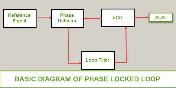
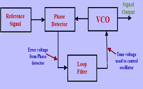
Therefore the highest feasible PFD frequency. September 2015 DocID15058 Rev 6 187 STM32F101x4 STM32F101x6 Low-density access line ARM-based 32 bit MCU with 16 or 32 KB Flash 5 timers ADC and 4 communication interfaces. Block diagram of a PLL.
PLL Ground is also connected to low voltage ground for core logic on 144LQFP pin 35. Leave a Reply Cancel reply. For other small form-factor package availability and marking information please visit.
DS41440 PIC16LF18251829 Data Sheet 1420-Pin Flash Microcontrollers. DS40001715 PIC16LF17048 Data Sheet 1420-Pin Flash 8-bit Microcontrollers.

Block Diagram Of Digital Pll Adopting A Lms Calibration Loop Download Scientific Diagram
Phase Locked Loop Operating Principle And Applications

Block Diagram Of The Phase Locked Loop Circuit Download Scientific Diagram
Phase Locked Loop Operating Principle And Applications
Phase Locked Loop Operating Principle And Applications

Fll Assisted Pll F Pll Loop Architecture Block Diagram Download Scientific Diagram

Pll Block Diagram Download Scientific Diagram

Simulation Block Diagram For A Classical Digital Phase Locked Loop On Download Scientific Diagram

Schematic Block Diagram Of The Pll Download Scientific Diagram

1 An Basic Block Diagram Of Pll Download Scientific Diagram

General Block Diagram Of Adpll Beginning Of All Digital Phase Locked Download Scientific Diagram

Block Diagram Of Pll 1 Download Scientific Diagram

1 Block Diagram Of A Phase Locked Loop Download Scientific Diagram
Block Diagram Of Phase Locked Loop Pll Download Scientific Diagram

Basic Diagram Of A Digital Pll Download Scientific Diagram

Block Diagram Of A 3 Rd Order Digital Pll Loop Filter Download Scientific Diagram

Block Diagram Of Conventional Dtc Based Digital Pll Download Scientific Diagram